


Semiconductors
Semiconductors are tiny chips that power almost everything electronic, from phones to cars. They're like the tools ("picks and shovels") that make modern industries run, driving big tech shifts like Industry 3.0 (computers and automation) and Industry 4.0 (AI, robotics, and smart devices).
History
1947: The Birth of the Transistor
The invention of the transistor, considered one of the most transformative technologies of the 20th century, was accomplished at Bell Laboratories by John Bardeen, Walter Houser Brattain, and William Shockley. This innovation became the foundation of modern electronics. Many would argue that this was the birth of Industry 3.0, defined by the rise of technologies such as semiconductors, programmable logic controllers (PLCs), computer-aided design (CAD), and early automation systems that transformed manufacturing through digitalization and precision.
1952-1956: Proliferation of Semiconductor Technology
In 1952, Bell Labs began licensing its transistor manufacturing technology, laying the groundwork for companies like Texas Instruments, IBM, Motorola, and Sony to enter the field.
By 1956, Bell Labs formally introduced lithography, diffusion, and oxidation layer mask technology during its third sharing of transistor technology. This critical advancement fueled the growth of Fairchild Semiconductor, Intel, AMD, and other future industry leaders, spurring innovation in the lithography space.
1958: The First Integrated Circuit
The concept of integrating multiple transistors onto a single circuit was first proposed in 1952 by Geoffrey Drummer.
On August 28, 1958, Jack Kilby of Texas Instruments created the first functional integrated circuit (IC) by wire bonding three transistors together, marking the birth of what is now called a System-in-a-Package (SIP).
Robert Noyce of Fairchild Semiconductor merged Jean Hoerni’s planar process with the IC concept, introducing the modern IC.
1956-1968: The Rise of Silicon Valley
The story of Intel's founding is the same as how Silicon Valley (SV) got its name. William Shockley, co- inventor of the transistor, started a company called Shockley Semiconductor Labs in 1956. SV is derived from the Silicon used in transistors and chips. A year later, the so-called traitorous eight, quit to start Fairchild Semiconductor, which quickly became the world's premier chip company. A decade later, two of the founders of Fairchild, Bob Noyce and Gordon Moore, left to start Intel. Back then, short term memory (RAM) or central processing unit (CPU) did not exist, these are both Intel's innovations. Gordon Moore, co-founder of Intel, established Moore’s Law - "the number of transistors incorporated in a chip will approximately double every 24 months" and has held true even till this day.
1960s-1970s: The Foundations of Lithography
In 1961, GCA Medical Technology Inc. built the first lithography machine, and in the 1970s, Kasper Instruments Inc. built the first lithography machine. Because the threshold of lithography technology was relatively low at that time, in the late 1960s, Nikon and Canon of Japan, because of the similarity of their industries, also started to set foot in the market. lithography industry.
1980s: The Glory Years for Japan
By the 1980s, Nikon released its first commercial stepper lithograph and served a series of large customers such as IBM, Intel, and AMD. By 1984, Nikon was able to equal GCA and served Ultratech, Eaton, P&E, Canon, Hitachi and a few others. This was the year that that ASML (Advanced Semiconductor Materials Lithography), the future dominant player in the lithography industry, was founded as a joint venture with Philips. The 1980’s were the glory years for the Japanese semiconductor and photolithography industries. In the late 1980s, Nikon and Canon maintained a duopoly, while ASML held 10% of the market.
1990s: The Birth of EUV Research
In the 1990s, Researchers at several United States Department of Energy (DOE) national laboratories (specifically Livermore, Berkeley, and Sandia) were funded to perform basic research into the technical obstacles of EUV, The Extreme Ultraviolet Limited Liability Company (EUV LLC) was formed and succeeded in the technology. Intel, Canon and Nikon (leaders in the field at the time), as well as ASML and Silicon Valley Group (SVG) all sought licensing, however Congress denied Japanese companies the necessary permission as they were perceived as strong technical competitors at the time and should not benefit from taxpayer-funded research at the expense of American companies. In 2001 SVG was acquired by ASML, leaving only a single company as the sole benefactor of the critical technology.
2018: ASML’s EUV Breakthrough
By 2018, ASML succeeded in deploying the EUV-LLC IP after several decades of developmental research, with incorporation of European-funded EUCLIDES (Extreme UV Concept Lithography Development System) and long-standing partner German optics manufacturer ZEISS and synchrotron light source supplier Oxford Instruments. This dwarfed competitors Nikon and Canon as they were denied IP access.
Before EUV, chip makers had three companies they could choose from for their photolithography tools: Canon, Nikon and ASML. Nikon is still a competitor for DUV, but ASML is the only option for EUV. Experts say it could take decades for any another company to catch up, not only because of ASMLs proprietary tech, but because its bult complex often exclusive deals with nearly 800 suppliers.
The Technology
What is a Chip?
A microchip, also known as a chip, computer chip, or integrated circuit, is a small, flat piece of silicon that contains thousands or even billions of tiny electrical circuits. These circuits allow the chip to perform tasks like processing data and controlling devices.
The process of making a microchip begins with silicon wafers. Silicon is the material of choice because it is a semiconductor, meaning its ability to conduct electricity can be controlled. By adding small amounts of other materials like phosphorus or boron, the silicon can be adjusted to control electrical currents, essentially turning them on or off. This is what enables chips to perform calculations and execute tasks.
To create the chip, purified silicon is first melted and sliced into thin, round pieces called wafers. These wafers serve as the base for building the chips. Once the wafer is ready, transistors—the key components in a chip—are built up in layers. Each transistor is like a tiny switch that can turn electrical signals on and off. The more transistors a chip has, the more powerful it can be.
The process of adding these transistors and circuits to the chip involves lithography. This is where light is used to "print" the tiny patterns of the chip onto the wafer. In lithography, light is projected through a mask containing the chip design. The wafer is coated with a special light-sensitive chemical called photoresist. When the light hits the photoresist, it creates intricate patterns that form the circuits and transistors on the chip.
This process is repeated, adding many layers to build up the full chip, with each layer adding new circuits that allow the chip to perform its functions. The end result is a microchip that can power everything from smartphones and computers to cars and appliances.
How Microchips Relate to CPUs, GPUs
CPU (Central Processing Unit):
The CPU is like the "brain" of a computer. It handles all the basic tasks, like running software, doing math, and managing the flow of information. CPUs are found in almost every device, including computers, phones, and servers. They’re great for doing one thing at a time quickly, like following a to-do list step by step.
GPU (Graphics Processing Unit):
GPUs are specialised microchips designed to handle large-scale parallel processing - doing many tasks at the same time. Originally built for rendering graphics and images in gaming and visual applications, they are now widely used in fields like artificial intelligence (AI), machine learning, and scientific simulations.
GPUs can process thousands of operations simultaneously, making them highly efficient for tasks requiring massive data computation.
The Evolution of Lithography: DUV to EUV
In the past, the light used for lithography was much bigger, and as the chips needed to get smaller, the light source also had to get smaller. Here’s how it progressed:
Visible Light (1960s-1980s)
In the early days of lithography, visible light was used. However, the wavelength of visible light was too large to produce the tiny features needed for modern microchips. This limited the size and performance of the chips that could be made.
DUV (Deep Ultraviolet) Lithography (1990s-2000s)
In the 1990s, the industry moved to DUV (Deep Ultraviolet) light sources, which had a much smaller wavelength of 248nm, and later 193nm. These shorter wavelengths allowed for the production of smaller transistors, which led to smaller, more powerful chips. With DUV technology, chips with transistors as small as 7nm or 5nm could be created, a significant leap forward.
EUV (Extreme Ultraviolet) Lithography (2010s-present)
The most recent advancement is EUV (Extreme Ultraviolet) lithography, which uses 13.5nm light. This is much smaller than the 193nm wavelength used in DUV machines, allowing for the production of even smaller transistors—down to 3nm or even 2nm. EUV has become essential for creating the latest-generation chips, offering increased speed, power efficiency, and performance.

Over time, lithography light sources have evolved significantly, starting with visible light in the 1960s, followed by the shift to DUV (Deep Ultraviolet) light in the 1990s, with wavelengths of 248nm and later 193nm. The next major leap was 193nm immersion lithography in the 2000s, which enhanced resolution by using liquid to focus light more precisely. Today, ASML's EUV (Extreme Ultraviolet) machines, utilizing 13.5nm light, represent the cutting edge of lithography, enabling the creation of the smallest, most powerful chips ever. These advancements have allowed ASML to dominate the high-end lithography market, leaving the infamous Japanese competitors like Nikon and Canon far behind.
This is where ASML, the world leader in lithography, plays a crucial role. Their Extreme Ultraviolet (EUV) lithography machines use light with a wavelength of 13.5 nm, significantly smaller than the 193 nm deep ultraviolet (DUV) used in previous generations. EUV light is so short it is invisible to the human eye and absorbed by natural materials, necessitating the process to be conducted in a vacuum. These machines are extraordinary feats of engineering, capable of producing 3,000 wafers per day, with hundreds of chips per wafer. Each chip can contain billions of transistors, thinner than a strand of human hair.
Node Size (nm)
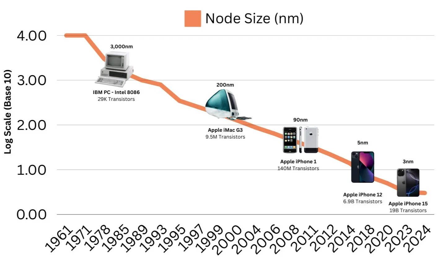
A smaller technology node means making the transistors on a chip. Transistors are tiny switches that control electricity flow, and shrinking their size makes them both faster (because electricity has less distance to travel) and more energy-efficient (because they use less power).
The size of a node is measured in nanometers (nm) — an incredibly tiny unit of length, equal to one-billionth of a meter (0.000000001m). To put it simply, the smaller the nanometer number, the more advanced and powerful the chip is. Looking back to IBM PC of 1981 that used an Intel 8086 chip, the node size was 3,000nm and had 29 thousand, fast forward to a recent iPhone 15 which has a node size of 3nm (1,000X smaller) and over 19 billion transistors.
Leading Node vs Trailing Node
Leading node process technology refers to the most advanced semiconductor manufacturing techniques, using extremely small transistors (such as 5nm and 3nm) to produce faster, more power-efficient chips. These cutting-edge nodes benefit from EUV (Extreme Ultraviolet) lithography, which allows for more precise patterning of extremely small features. This precision is crucial for high-performance devices that require large numbers of densely packed transistors. Devices like Apple’s A17 Bionic chip (used in the iPhone 15) and NVIDIA’s A100 GPUs (used for AI and machine learning applications) are examples of products made using leading nodes. These chips rely on the enhanced performance and efficiency offered by smaller node technologies, which is why they're ideal for smartphones, AI processors, and high-end computers.
On the other hand, trailing node process technologies (such as 22nm or older) often use DUV (Deep Ultraviolet) lithography. While DUV is not as precise as EUV, it is more cost-effective and sufficient for creating chips where extreme performance and transistor density are not critical. These trailing nodes are used in applications like Internet of Things (IoT) devices, automotive electronics, and other consumer products where lower cost is a priority. For example, microcontrollers used in smart home devices and automotive chips for basic vehicle control systems typically rely on trailing node technologies. These chips don’t require the same level of precision and transistor density as the advanced chips in smartphones or AI hardware.
The Supple-Chain
The semiconductor ecosystem is a very complex end-to-end technology value chain that requires tight integration between different semiconductor companies, each company possess a unique set of specialized capabilities and focus on only one part of the value chain. To think about the role of semiconductors and the players in the industry, let´s deconstruct the value chain and work backwards from the end use of the product, for example, a smartphone sold by Apple. A smartphone has many chips inside of it, these chips are designed by fabless companies that only design and sell hardware devices such as Nvidia, AMD, Qualcomm, etc. Once designed, the semiconductor chips are manufactured by a foundry, a semiconductor company with fabrication plants, also known as “fabs”, from companies such as TSMC, Intel or Samsung. The fabrication plants use high-tech machinery, in this case EUV lithography machines sold by ASML, to manufacture semiconductor chips.
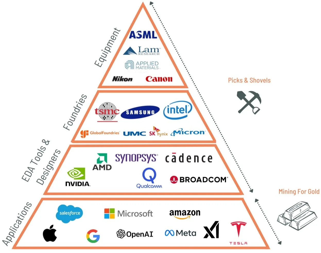
Foundries – “fabs”
Also known as fabrication plants, physically build semiconductor chips
“Fabless”
Design and market semiconductor chips but do not own or operate their own fabrication facilities.
Equipment
ASML is the undisputed leader in the semiconductor tool market, particularly in the area of Extreme Ultraviolet (EUV) lithography, holding a total monopoly in EUV with its machines accounting for 100% of the global market share in this advanced technology. EUV is essential for producing the smallest, most advanced chips at nodes such as 5nm, 3nm, and below. In contrast, competitors Nikon and Canon remain focused on Deep Ultraviolet (DUV) lithography, which is still used for less advanced nodes, but they have been unable to develop EUV technology, leaving ASML with a dominant position in the high-end market. While Nikon holds around 20% of the DUV market share and Canon has about 10%, ASML leads with 70% of the DUV market share, further solidifying its position.

ASML relies on a vast network of more than 5,000 suppliers to manufacture its EUV machines, which is made up of seven different modules, each built at one of ASMLs six manufacturing sites among its 60 locations around the world, then shipped to reassembled to Veldhoven for testing. Then it is disassembled again for shipment, using 20 trucks and three fully loaded 747s.
ASML’s EUV machines fall into two main categories:
TWINSCAN NXE Series: These are the current production workhorses, including models like the NXE:3400C and NXE:3600D, which are used for nodes such as 5nm and 3nm.
TWINSCAN EXE Series (High-NA EUV): These next-generation machines, including the EXE:5000 and EXE:5200, will enable chip production below 2nm by offering even greater precision.
The technology behind these machines is incredibly expensive, with TWINSCAN NXE models costing over $200 million each. The High-NA EUV machines (EXE series) are even more costly, with prices estimated at over US $400 million. Due to the high price tag and the complexity of operating these machines, only a few companies can afford them. The largest players in the semiconductor industry, including TSMC, Samsung, Intel, SK Hynix, and Micron, are the primary customers. Together, TSMC, Samsung, and Intel account for over 80% of ASML’s business, underscoring the importance of these companies in driving the demand for advanced chip manufacturing.
Other tool providers like Lam Research and Applied Materials play key roles in semiconductor fabrication, focusing on processes like etching, deposition, and chemical treatments. However, these companies do not compete directly in the EUV space, which remains ASML's domain. Overall, ASML’s control of EUV and its role in advancing chip technology ensure its continued dominance in the semiconductor tooling market.
ASML's rise to dominance in EUV was the result of decades of investment in research and the development of cutting-edge technology. The financial resources required to sustain the development and operation of these tools act as significant barriers to entry. Even companies with substantial financial backing, like Niko and Canon, faced immense challenges and abandoned their EUV lineup years ago, leaving ASML to dominate. While alternative methods for achieving 7nm node sizes without EUV have been announced, they would not be as effective as the EUV-based solutions, reinforcing the necessity of ASML's technology in the production of advanced chips.
EUV Lithography and the Department of Energy - ASML
The development of EUV lithography was shaped by U.S. government funding through the Department of Energy (DOE), which supported key research in the 1990s and 2000s. ASML gained a critical edge by acquiring U.S.-based companies like Chromatica and Advanced Lithography, securing vital patents and technology for EUV. Meanwhile, Nikon and Canon, despite leading in DUV lithography at the time, couldn't access these U.S.-developed technologies due to patent restrictions enforced by the U.S. government, allowing ASML to become the only company with the ability to produce and commercialize EUV lithography machines.
Foundries
TSMC’s dominance in the semiconductor foundry market stems from its technological leadership, focus on advanced manufacturing nodes, and specialization in the foundry business. With over 60% of the global market share and more than 80% of the 5nm and 3nm node market, TSMC has attracted major clients like Apple, AMD, and Nvidia by consistently delivering cutting-edge chip technologies. Unlike Samsung, which is spread across various businesses like memory and displays, or Intel, which has only recently expanded its foundry operations, TSMC’s singular focus on chip manufacturing has allowed it to invest heavily in R&D and production capacity. Its strong customer relationships, ecosystem advantages, and reliable manufacturing capabilities have helped it maintain a dominant position, while competitors struggle to match its pace in advanced nodes.
Samsung, the second-largest foundry with around 11% market share, remains a strong competitor but is more focused on both manufacturing and memory, limiting its foundry capacity. Intel, with 6% of the market, is working to expand its foundry business but lags behind TSMC in technological advancements. Other key players like GlobalFoundries and UMC also compete but do not offer the advanced nodes that TSMC leads in, reinforcing its market dominance.
Design / EDA Tools
Chip designers and Electronic Design Automation (EDA) tool providers serve distinct but interconnected roles in the semiconductor industry. Chip designers like NVIDIA, AMD and Qualcomm focus on creating blueprints and architectures for specialised semiconductor devices such as GPUs, CPUs, and AI processors. They rely on the software and automation provided by EDA tool providers—companies like Synopsys, Cadence, and Siemens (Mentor Graphics)—to design, simulate, verify, and optimize these chips. EDA tools streamline complex tasks such as schematic capture, physical layout, timing analysis, and power optimization, enabling designers to meet power, performance, and area (PPA) requirements. Once designs are finalized, chip designers send them to foundries like TSMC for fabrication. EDA providers thus play an enabling role, offering essential technology that powers the innovative designs developed by chip companies.
Outlook
The semiconductor manufacturing equipment market, which includes tools essential for chip production, is valued at approximately $110.5 billion in 2024, with projections to reach $175.2 billion by 2030, growing at a compound annual growth rate (CAGR) of 7.9% (Grand View Research, Fortune Business Insights). Similarly, the semiconductor foundry market is expected to continue expanding, with a forecasted size of $110 billion by 2025, driven by the demand for advanced node manufacturing in sectors like telecommunications, consumer electronics, and automotive, with a CAGR of 8.5% from 2024 to 2030 (IC Insights, Fortune Business Insights). The electronic design automation (EDA) tools market, which supports chip design, is valued at $13 billion in 2024 and is expected to grow at a strong 9.6% CAGR through 2030, driven by the increasing complexity of designs needed for cutting-edge technologies such as AI and advanced computing (Markets and Markets, Grand View Research).
Growth Drivers
The semiconductor industry is set to benefit from several long-term secular tailwinds, including advances in key technologies like AI, 5G, edge computing, and automotive developments. Over the next decade, the semiconductor market is expected to double from about $450 billion in 2019 to $1-1.3 trillion by 2030, with a compound annual growth rate (CAGR) of 6-8% (Allied Market Research & McKinsey & Company).
Key growth drivers include automotive electrification, where electric vehicles (EVs) are expected to comprise 70% of car sales by 2030, significantly increasing semiconductor content in vehicles (McKinsey & Company). The shift to autonomous vehicles (AVs) will require advanced chips for high-level computation (Allied Market Research).
Artificial Intelligence (AI) and machine learning (ML) are another critical catalyst, with the AI chip market projected to grow at a CAGR of 45%, reaching US$91 billion by 2025 and US$130 billion by 2030 (Allied Market Research).
Additionally, 5G technology is driving demand for higher-capacity, more efficient chips to support wireless infrastructure, with expectations for edge computing and hyperconnectivity to grow at similar rates (Allied Market Research & McKinsey & Company).
The shift from leading node to trailing node process technology continues to define semiconductor manufacturing, with leading-edge chips enabling advancements in 5G, IoT, edge AI, and cloud computing (McKinsey & Company). These innovations are essential for high-speed mobile devices, autonomous vehicle systems, and data centers, where reducing power consumption and increasing processing power are critical for future growth (Allied Market Research). The global semiconductor industry has matured from its volatile past, with increased discipline and consolidation leading to a few dominant players who drive innovation across these diverse sectors (Allied Market Research).
Further supporting growth, the push for technological sovereignty and government investments in semiconductor manufacturing capacity are expanding production and reducing supply chain risks. For example, the US has passed the CHIPS Act, with $52 billion in federal support, while South Korea and Japan are investing billions in R&D and facilities to strengthen their semiconductor ecosystems (Allied Market Research & McKinsey & Company).
These developments, paired with the growing demand across various end-markets like datacenters, consumer electronics, and industrial robotics, are expected to propel the industry’s robust growth trajectory well into the next decade (McKinsey & Company).